DATA SHEET www.onsemi.com This is a complete series of 5 Watt Zener diodes with tight limits and ... Zener Voltage Range − 3.3 V to 200 V.
n b d
Rev. 2.4 25-Nov-2021. 1. Document Number: 85607. For technical questions within your region: DiodesAmericas@vishay.com
bzx
25 nov. 2021 Silicon planar power Zener diodes. • For use in stabilizing and clipping circuits with high power rating. • Standard Zener voltage tolerance ...
n a
Three complete series of Zener diodes are offered in the convenient surface mount plastic SOD−123 package. this data sheet. DEVICE MARKING INFORMATION.
mmsz bt d
Silicon planar Zener diodes. • The Zener voltages are graded according to inaccuracies or incompleteness contained in any datasheet or in any other.
bzt
See detailed ordering and shipping information on page 3 of this data sheet. ORDERING INFORMATION. Page 2. 1N5221B − 1N5252B www.onsemi.
n b d
Silicon epitaxial planar diode. • Electrically equivalent diodes: inaccuracies or incompleteness contained in any datasheet or in any other.
n
N-channel 1050 V 6 typ.
https://www.st.com/resource/en/datasheet/stfw2n105k5.pdf
How to select a Surge Diode
understanding of how to select a TVS diode for surge protection which will directly When reading a TVS diode data sheet
This complete new line of 3 W Zener diodes offers the following this data sheet. ... 12V. 6.8V. Rating and Typical Characteristic Curves (TA = 25°C).
smb bt d
245815

⬧ Semiconductor Components Industries, LLC, 2018
April, 2021 Rev. 41Publication Order Number:
1N5221B/D
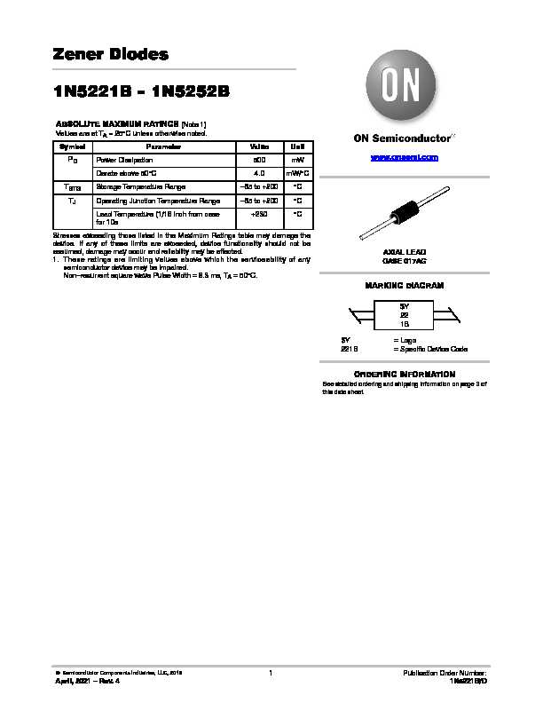
Zener Diodes
1N5221B - 1N5252B
ABSOLUTE MAXIMUM RATINGS (Note 1)
Values are at T
A = 25°C unless otherwise noted.
Symbol
ParameterValueUnit
P D
Power Dissipation500mW
Derate above 50°C4.0mW/°C
T
STGStorage Temperature Range65 to +200°C
T J Operating Junction Temperature Range65 to +200°C
Lead Temperature (1/16 inch from case
for 10s+230°C Stresses exceeding those listed in the Maximum Ratings table may damage the device. If any of these limits are exceeded, device functionality should not be assumed, damage may occur and reliability may be affected.
1. These ratings are limiting values above which the serviceability of any
semiconductor device may be impaired.
Nonrecurrent square wave Pulse Width = 8.3 ms, T
A = 50
°C.www.onsemi.com
MARKING DIAGRAM
AXIAL LEAD
CASE 017AG
$Y = Logo
221B = Specific Device Code$Y
22
1BSee detailed ordering and shipping information on page 3 of
this data sheet.
ORDERING INFORMATION
1N5221B 1N5252B
www.onsemi.com 2
ELECTRICAL CHARACTERISTICS Values are at T
A = 25°C unless otherwise noted.
Device
V Z (V) @ I Z (Note 2) Z Z (?) @ I Z (mA)Z ZK (?) @ I ZK (mA)I R (A) @ V R (V)T C (%/?C)Min.Typ.Max.
1N5221B2.2802.42.5230201,2000.251001.00.085
1N5222B2.3752.52.62530201,2500.251001.00.085
1N5223B2.5652.72.83530201,3000.25751.00.080
1N5225B2.8503.03.15029201,6000.25501.00.075
1N5226B3.1353.33.46528201,6000.25251.00.070
1N5227B3.4203.63.78024201,7000.25151.00.065
1N5228B3.7053.94.09523201,9000.25101.00.060
1N5229B4.0854.34.51522202,0000.255.01.0±0.055
1N5230B4.4654.74.93519201,9000.255.02.0±0.030
1N5231B4.8455.15.35517201,6000.255.02.0±0.030
 ⬧ Semiconductor Components Industries, LLC, 2018